- Heated ion implantation technology realizes low resistance of an ultra-thin fin -
Wataru Mizubayashi (Senior Researcher) and Meishoku Masahara (Leader), Silicon Nano-Device Group, the Nanoelectronics Research Institute (Director: Seigo Kanemaru) of the National Institute of Advanced Industrial Science and Technology (AIST; President: Ryoji Chubachi), in collaboration with Nissin Ion Equipment Co., Ltd. (President: Nobuo Nagai), have developed a low-resistance source/drain formation technology that can be applied in the finFETs of 14-nm generation and beyond.
The greatest issue for the finFETs of 14-nm generation and beyond was low-resistance source/drain formation on the ultra-thin (10 nm or less) silicon fin. Lower resistance is usually obtained by ion implantation of impurities, but on the fin part, crystal defects that occur during the implantation end up increasing the resistance. Since these crystal defects are difficult to resolve, the result has been that lower resistance is difficult to realize. The heated ion implantation technology developed in the present research is capable of implanting impurity ions in the ultra-thin fin part without causing crystal defects to occur, achieving lower resistance. It has also significantly increased finFET reliability. The developed technology is contributing to the resolution of the issue of low-resistance source/drain formation in the finFETs of 14-nm generation and beyond.
Details of this technology will be presented at the International Electron Device Meeting (IEDM) to be held on December 9 to 11, 2013 in Washington, D.C., USA.
 |
|
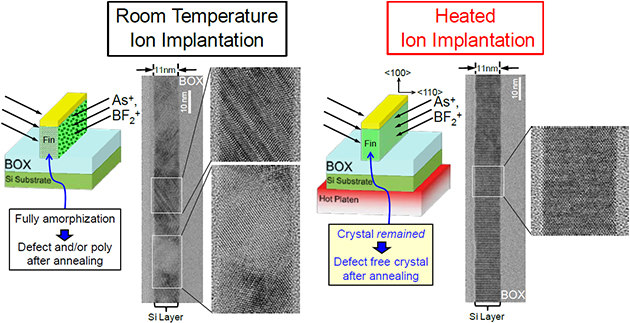
Schematic illustrations of room-temperature ion implantation and heated ion implantation, and crystallinity of ultrathin silicon layers after activation annealing
In illustrations, BOX is silicon dioxide (SiO2), As+ is arsenic ion, and BF2+ is boron difluoride ion. |
Silicon integrated circuits have realized increasingly advanced performance and integration to date by miniaturizing the transistor elements that are the smallest components of those circuits. The miniaturization of these elements is also linked to cost reduction, and there is intense on-going competition in the development of miniaturized elements. For the technology of 14-nm generation and beyond transistors that are anticipated to enter the market in 2017 and after, however, the greatest issue is the emergence of the influence of source/drain resistance at the ultra-thin fin part. Since increased resistance is a factor in degradation of transistor performance, there is great demand for technology for forming low-resistance source/drain areas.
AIST has been pursuing research and development of the transistors with a new structure called finFETs. In 2003, AIST developed a four-terminal finFET capable of independent gate control and demonstrated its ability to electrically control the threshold voltage (Vth) (AIST press release on December 9, 2003). In 2012, an amorphous metal was used for the gate electrode, instead of the usual polycrystalline metal gate electrode, in order to reduce the variability in Vth. A significant reduction in variability was achieved (AIST press release on December 12, 2012). Research and development in process technology is presently proceeding with the aim of further improving finFET performance.
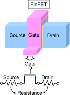
Figure 1 shows a schematic illustration of a finFET. When the source/drain resistance is high, there will be a marked voltage drop when the transistor operates. This lowers the drain current, which is an indicator of performance. Achieving a high-performance finFET will require the technology for low-resistance source/drain formation. The general method of source/drain formation is by ion implantation of impurities followed by annealing to activate the implanted impurities. With this method, however, there is an issue with increased source/drain resistance in the ultra-thin fin part.
 |
|
Figure 1 : Schematic illustration of FinFET and source/drain resistance |
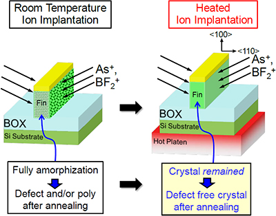
Figure 2 shows a schematic illustration of a comparison between conventional room-temperature ion implantation and the newly developed heated ion implantation. In the case of conventional room-temperature ion implantation, the entire fin part becomes an amorphous layer after ion implantation. Since a crystal layer is virtually absent, the following activation annealing produces crystals or polycrystals that contain many defects, and the result is increased resistance. Heated ion implantation is available as a method for maintaining the crystal layer even after ion implantation. Although the crystal layer in the fin part can be maintained by the heated ion implantation, this approach results in more defects than room-temperature ion implantation. With conventional planar transistors, either crystal recovery does not occur or defects remain even after the annealing is carried out following heated ion implantation, resulting in degradation of transistor performance. Therefore, heated ion implantation was not used for planar transistors. In the case of the finFET, however, the fin layer is so thin that defects caused by the heated ion implantation are removed from the fin by the annealing, and the issue of remaining defects can be resolved. As shown in Fig. 2, when the heated ion implantation is used with finFETs, the annealing eliminates defects, so that the defect-free crystal can be recovered and the resistance is therefore significantly reduced. In other words, the heated ion implantation can be expected to enable defect-free and low-resistance source/drain formation.
 |
|
Figure 2 : Schematic illustration of room-temperature and heated ion implantation for source/drain in FinFETs |
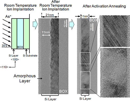
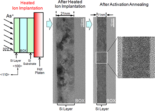
Room-temperature ion implantation and heated ion implantation were carried out on ultra-thin silicon layers under the same conditions as for finFET source/drain fabrication, and the effects on the crystalline state of the silicon layer were examined (Figs. 3 and 4). First, in the case of room-temperature ion implantation, ion implantation into a 21-nm silicon layer resulted in the production of an 11-nm amorphous layer (Fig. 3). Next, a test sample with completely amorphous 11-nm silicon layer was fabricated and subjected to annealing. Crystal recovery could not occur because there were no crystalline portions, which work as the necessary seeds for recovery of crystal in the silicon layer, and polycrystals, twin crystals, and so on formed instead (Fig. 3). This causes source/drain resistance to increase.
 |
|
Figure 3 : Crystallinity of silicon layer before and after activation annealing in room-temperature ion implantation |
The heated ion implantation was performed at an implantation temperature of 500 ℃. A crystalline film was maintained throughout the entire silicon layer even after the ion implantation (Fig. 4). The crystalline film serves as the seed required for crystal recovery, so that crystal recovery did take place after annealing even with an ultra-thin 11-nm silicon layer, and the resulting crystalline film was free of defects. This contributes to the reduction of source/drain resistance, which means that the heated ion implantation can enable defect-free and low-resistance source/drain formation.
 |
|
Figure 4 : Crystallinity of silicon layer before and after activation annealing in heated ion implantation |
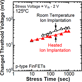
Next, the influence of heated ion implantation on finFET reliability was evaluated (Fig. 5). Reliability was evaluated by the change over time in the threshold voltage when a constant voltage was applied to the gate. The change in threshold voltage of the finFET fabricated using the heated ion implantation was smaller than that of the finFET fabricated using the room-temperature ion implantation, indicating that the reliability had increased. In other words, high-reliability finFETs can be fabricated using the heated ion implantation. These results indicate that the heated ion implantation is a promising technology for source/drain formation in the fin parts of the finFETs of 14-nm generation and beyond.
 |
|
Figure 5 : Time dependence of threshold voltage by constant voltage in FinFETs proceeded with room-temperature ion implantation or heated ion implantation |
In the future, the researchers will optimize finFET manufacturing processes and develop mass-production equipment with the aim of applying the heated ion implantation in mass-production finFET manufacturing processes.