- New industrial ink-jet technology enables low-resistance wiring on various types of substrates -
Jun Akedo (Principal Research Scientist and concurrently Leader of the Integration Process Technology Group) and Akito Endo (Post-Doctoral Research Scientist), the Advanced Manufacturing Research Institute (Director: Norimitsu Murayama) of the National Institute of Advanced Industrial Science and Technology (AIST) (President: Tamotsu Nomakuchi) have succeeded in developing a high-speed printing technology that involves laser irradiation during ink-jet printing. The line width is scaled down while the line thickness is increased. Fine conductor patterns less than 10 µm in line width are successfully printed at a speed of 10 mm/sec without reprinting and with an aspect ratio (thickness/width) higher than unity. This is what has been difficult to be realized using existing industrial ink-jet technologies. It is confirmed that our newly invented laser-assisted ink-jet printing (LIJ) technology can print thin wires with a high aspect ratio by using ultrafine metal particle ink on various types of substrates regardless of substrate surface conditions such as steps of up to several hundred µm, material and roughness.
The wire (10 µm in line width) produced by the LIJ technology has a resistance per unit length of as low as 6 Ω/cm due to the high aspect ratio. This is a great improvement over the existing industrial ink-jet printing technologies using ultrafine metal particle ink where the interconnection resistance would typically be 70 Ω/cm for a line width of 10 µm.
Using the developed technology, low-resistance wires can be printed at high speed for the interposers between chips and a main board, wiring on flexible resin members, step connections between metal parts, and high-density wiring on curved surfaces. The technology will greatly improve the efficiency of development and production of microelectronic devices.
 |
|
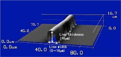
Fine wire with high aspect ratio (thickness/width) |
Today's diversified product specifications and continuously decreasing product cycles in electronic device manufacturing require on-demand design and production technologies that can bring about high-mix low-volume production as well as downsizing and cost reduction. When electronic devices are built into the final product, they must be securely mounted without the slightest damage to the device characteristics; thus a significant part of the device cost is due to the assembly process. Furthermore, the existing semiconductor micro-processing technology is becoming increasingly difficult to apply to such large-area devices as flat panel displays (FPDs) because the vacuum processes for large-area devices are very expensive. Due to these factors, especially in the area of electronic part mounting, expectations are raised for the evolution of printed electronics technology that uses ink-jet printing and produces wires at atmospheric pressure without masks.
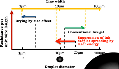
However, in printing fine patterns using existing industrial ink-jet technologies, the narrowest achievable line width remains at roughly 30–50 µm, considering also the yield, because the viscosity of ink must be controlled to reduce the ejected ink droplet size, and such processes as substrate surface treatment and fine mask pattern fabrication are additionally needed. Moreover, there is also a serious problem with fine pattern wires thus produced: the wire becomes too thin (aspect ratio becomes too low) because ink droplets tend to spread and droplets themselves are small; especially in the case of conductor wiring, repeated reprinting is needed to obtain practically small interconnection resistance, which greatly degrades the production efficiency. Therefore, new ink-jet technology has been desired for quickly printing low-resistance fine metal patterns (Fig. 1).
 |
|
Fig. 1 Range of line width and interconnection resistance against the diameter of ejected ink droplets |
AIST has been developing a high-aspect-ratio ink-jet printing technology for reduced line width and increased line thickness, based on the expectation that an ink-jet technology for high-mix low-volume production would become more important for the highly integrated high-density mounting of electronic devices including MEMS and LSI chips. Instead of simply reducing the nozzle size and improving the ink material, we targeted the suppression of ink droplet spread after landing, which was previously believed to be too technically difficult to achieve, so that low-resistance fine wires could be printed even on uneven substrates.
This study was undertaken as part of the "Highly Integrated, Complex MEMS Production Technology Development Project (2006-2008): MEMS/semiconductor horizontal fine-pitch wiring technology; High-density low-temperature laminating and integrating packaging technology," sponsored by the New Energy and Industrial Technology Development Organization (NEDO).
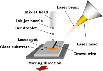
In this study, ink droplets with a diameter ≈25 µm (8.2 picoliters) are ejected through a single-nozzle ink-jet head. The droplets are larger than those of a typical home-use ink-jet printer. CO2 laser is irradiated for local heating (Fig. 2) to control the fluidity of droplets and to accelerate evaporation of the solvent. Fine silver (Ag) wires with an aspect ratio higher than unity, line width of 5–10 µm, which is smaller than the ejected droplets, and line thickness of 10 µm (Fig. 3 and Fig. 4), are printed directly onto glass substrates. Wires with small line width and high aspect ratio are obtained without repeated printing, and the wires are printed at a greatly improved speed of 10 mm/sec per nozzle. This is the first report demonstrating the possibility of obtaining a line width even smaller than the diameter of an ejected ink-jet droplet. On a substrate without surface treatment, as shown in Fig. 3, we observed more than 250-fold improvement in aspect ratio over wires printed by the conventional industrial ink-jet technique without laser irradiation. Furthermore, we were able to effectively suppress both non-uniform spreading of droplets after landing (bulge effect) and non-uniform line thickness distribution (coffee ring effect). Using commercially available ink, in which silver nanoparticles are dispersed in organic solvent, the resistance per unit wire length is greatly reduced from 70 to 6 Ω/cm due to the laser irradiation for Ag patterns with a line width of 10 µm. In reducing the resistance of fine wires made by using ultrafine metal particle ink, improvement of the 'resistivity' of the wire has some limit; the resistance can be further reduced by increasing the aspect ratio, namely thickening the wire.
 |
|
Fig. 2 Laser-assisted ink-jet printing technology |
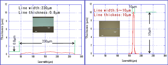 |
Fig. 3 Effect of laser irradiation on the aspect ratio (thickness/width) of printed wires
(left) Without laser irradiation (right) With laser irradiation |
Figure 5 shows a wire on a silicon substrate with steps, clearly demonstrating the advantage of the laser-assisted ink-jet printing (LIJ) technology. Due to the relatively large droplets, we were able to make the distance between the nozzle and substrate larger than that for existing ink-jet printing techniques; this contributed to the success of wire printing over steps exceeding 100 µm on silicon substrate. We had another issue related to surface roughness. As Fig. 6 (left) shows, in conventional ink-jet printing, the printed pattern tends to spread due to the capillary action along the in-plane direction of the substrate with fine surface irregularities. On the other hand, in LIJ printing, as shown in Fig. 6 (right), the droplets reaching the substrate are instantly solidified, and fine line printing is not affected by the surface roughness. It is confirmed that we were able to purposely create surface roughness so that the physical anchoring effect improved the adherence between the printed pattern and the substrate.
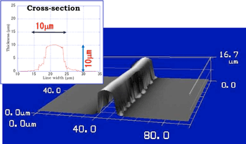
Fig. 4 High aspect ratio wire and its cross section |
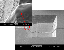
Fig. 5 Metal wire going over large steps on silicon substrate
|
A simple way of drying ink droplets is to heat the substrate. However, the heat from the substrate dries the opening section of the ink nozzle, and the nozzle easily becomes clogged; the heat creates a convective flow and causes the flying droplets to veer from their orbit, and so we cannot obtain good landing accuracy. Another known way to help dry the ink droplets is to increase the surface area against the volume of a droplet (Fig. 1). This is achieved by reducing the size of droplets down to sub-femtoliter ranges. However, if the opening section of a nozzle for ejecting droplets must be made small, the nozzle easily becomes clogged due to dried ink. On the other hand, in the newly invented LIJ technology, we can use a nozzle opening for several picoliters droplets, which is relatively large for printing fine wires, and we have much less local heating that could make the nozzle opening dry or cause the flying droplets to veer from their orbit; we have much less chance of having a clogged nozzle due to dried ink and can secure an accurate landing position for a droplet. Therefore, the technology contributes both practicality and accuracy to fine pattern printing.
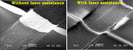 |
Fig. 6 Printed wires going over the groove formed by grinding the glass substrate
(left) Without laser irradiation (right) With laser irradiation |
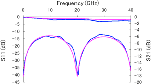
Fig. 7 Transmission characteristics of a high-frequency coplanar waveguide (<40 GHz)
Blue: measurement; Pink: theory |
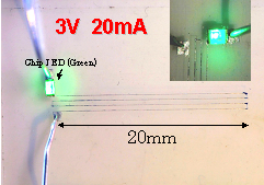
Fig. 8 Lighting test of an LED chip using the wire printed using LIJ technology (Width 30 µm; Length 80 mm) |
It is further confirmed that by using the newly developed LIJ technology, two-dimensional conductor patterns and conducting wires without post annealing can be printed; as Fig. 7 shows, a high-frequency coplanar waveguide can be fabricated with good transmission characteristics up to 40 GHz; as Fig. 8 shows, fine Ag wire patterns with a line width of 30 µm and length of 80 mm can be fabricated for lighting an LED with sufficient brightness using a rated current of 20 mA. The improvement in aspect ratio is also confirmed for many other ink materials, including oxides, due to the same laser irradiation effect as proven in the conductor material.
At AIST, we intend to improve the LIJ technology by optimizing the laser irradiation conditions and ink materials for finer patterns and by investigating the applicability to a multi-nozzle head. Furthermore, we will call for collaborative development with private companies so that the technology can be applied to a wide range of materials and applications. Through these efforts, the assembly cost will be greatly reduced and the adaptability for design specification changes and custom-fabrication will be improved.