The Institute of Scientific and Industrial Research, Osaka University, the National Institute of Advanced Industrial Science and Technology (AIST), and Japan Science and Technology Agency (president, Noriki Okimura) have jointly succeeded in the development of a production process for a new carbon nanotube transistor (CNT transistor), and thereby succeeded in the development of a CNT transistor with an operational stability 1000 or more times that of conventional CNT transistors.
The gain of CNT transistors is 10-100 times that of the silicon transistors used for present day integrated circuits, and thus they hold promise as the next generation of transistors.
However, conventional CNT transistors have the disadvantage that their characteristics vary significantly with time and voltage, resulting in a big obstacle to practical use.
It has been considered that this transistor instability is caused by contamination due to water and oxygen adsorbed on the CNT surface. Osaka University and the AIST have jointly found that photoresist residues may also be one of the causes, and have succeeded in the development of a new production technique enabling the removal of the factors inducing the variation of the characteristics. Using this technique, the time variation of the characteristics can be reduced to within 0.01 %, and a hysteresis in the characteristics can be almost completely removed, realizing sufficient operational stability for practical use.
By the technique we have developed, reliable CNT-transistors can be produced, enabling highly-sensitive biosensing and the detection of single biomolecules.
Because CNTs take fine tube-like structures of several nanometers in diameter, the application of CNTs to nano-electronic devices has been desired. Accordingly, various techniques for their utilization have been developed. In particular, field effect transistors (FETs) with a CNT channel have performance 10-100 times higher than conventional silicon field effect transistors (Si-MOSFET), and thus there has been active research and development into them as next-generation transistors. Development aimed at applications to the medical field, such as biosensors utilizing the high performance of CNT-FETs, has also been carried out.
However, conventional CNT-FETs have crucial disadvantages in transistor characteristics in that the electric current significantly fluctuates with time, sometimes resulting in current variations of several tens %. In addition, their current-voltage characteristics exhibit a hysteresis, that is, the current value is not uniquely determined by the applied voltage value, but depends on the history of the voltage change. For this reason, CNT-FETs can not be used in practical applications.
Stable CNT-FETs have been strongly desired for practical use. The cause of the transistor instability was considered to be due to water and oxygen adsorbed on the CNT surface, but even when they were completely removed from the surface, characteristics stable enough for practical use could not be achieved.
Aiming at the achievement of stable operation of CNT-FETs, Osaka University and the AIST have jointly investigated the cause of the instability.
This study was carried out under the "Strategic Promotion of Science and Technology" project funded by the Japan Science and Technology Agency, Osaka University and the AIST.
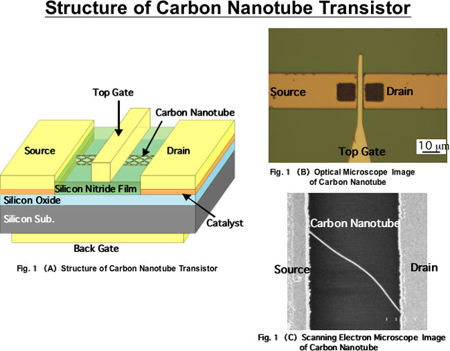
Figure 1(A) shows a structural illustration of a CNT-FET we have produced, in which the CNTs are formed on a silicon oxide thin film/silicon substrate, and source- and drain-electrodes, made of metal, are formed on both ends of the CNT region to take out the electric current. Furthermore, it should be noticed that the surface of the CNTs are covered with a silicon nitride thin film. Furthermore, on the silicon nitride thin film, the top gate electrode, being capable of controlling the electric current flowing in the CNTs, is formed. On the rear side of the silicon substrate, the back gate, similarly controlling the electric current, is formed. Figure 1(B) shows an optical microscopic image of a CNT-FET we have developed. In this image, each metallic electrode is visible, while the CNTs are not visible, because they are formed under the gate electrode. Figure 1(C) shows a scanning electron microscopic image of a CNT between the electrodes.
 |
The important points in this work are shown in Figure 2. Many amounts of not only water and oxygen in the air but also photo resist residues appearing in the production process adsorb on the CNT surface, as shown in Figure 2(A). These impurities can give electrons to the CNTs and take electrons out of them, resulting in a large time-variation of the electric current and a hysteresis in voltage-current characteristics of the CNT-FETs. Until now, complete removal of the photoresist residues has not been successful. In this work, we have developed a production process for making the CNT surface water-, oxygen-, and photoresist residue-free. Using this technique, and covering the CNT surface with a protective film, we have enabled the complete removal of the impurities from the CNT surface.
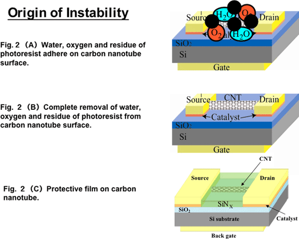 |
Figure 3 shows the time dependence of the electric current for a CNT-FET produced using a conventional method and a CNT-FET we have produced using our techniques. The electric current for the conventional CNT-FET exhibits a time-variation of 20 %. On the other hand, the CNT-FET we have produced shows almost no time variation in the electric current. The calculated variation is 0.01%, indicating that the operational stability of our CNT-FET is 1000 times or more that of the conventional CNT-FET.
Figure 4 shows the voltage dependence of the electric current for both CNT-FETs. For the conventional CNT-FET, when the applied voltage is increased from -5 to +5 volts, and then decreased from +5 to -5 volts, the voltage-current curve exhibits a hysteresis characteristic of 2-3 volts, while our CNT-FET exhibits no hysteresis in the current-voltage characteristic.
In this way, we have succeeded in the removal of time- and voltage-instability of the CNT-FET produced using our techniques. Thus, we think that the reliability of CNT-FETs will be greatly advanced using our techniques, and the application of the CNT-FETs to various electronic devices is promising.