The Center for Applied Near-Field Optics Research (CAN-FOR) of the National Institute of Advanced Industrial Science and Technology (AIST), one of independent administrative institutions, has successfully developed and manufactured on trial basis, a precision pit measuring system for optically inspecting error pits in the optical disk master and the optical ROM disk, and for assessing the pit geometry in nanometer accuracy, in collaboration with the Seiko Instruments Inc. (SII), first in the world. The development of this system has made it possible to clarify the correlation between the error signals and the pit geometry, not available heretofore, as well as to inspect the optical disk master and the optical ROM disk through simple means and with high accuracy. The system can be applied also to the development of ultra-high density optical disk master of 100 GB capacity and to the production line of the optical ROM disk.
Currently, the optical inspection is being used in the production of optical disk masters and optical ROM disks, but the conventional optical method can read error signals only from these disks, but is not able to identify the pit geometry, for instance. As the pit geometry in the optical disk masters and the optical ROM disks is strongly related to the optical signals, it is critically important to observe the pit geometry responsible to error signals with high accuracy. Error pits are supposedly produced through multiple causes, such as disk materials and fabrication process. It is indispensable, therefore, for upgrading the manufacturing process to clarify the causes for error generation and to feed back the information to the production line. In the commercially available optical disk masters and optical ROM disks, the pit size is greater than 400 nm, while that in the 100 GB optical disk master may be in the order of tens of nanometers, requiring pit accuracy as fine as 1 nm. For achieving the development of 100 GB optical disk master, it is essential to identify the correlation between the error signal and the pit geometry, and to monitor the pit geometry with fine accuracy.
A currently available optical disk master or optical ROM disk contains 1010 pits, and the number in a 100 GB optical disk master is supposed to be dozens of times as many. Until now, it has been thought impracticable to select error pits out of the optical disk master or optical ROM disk, because of enormous number of pits. In case of ultra-high density 100 GB optical disk master, however, with dozens of time as many pits, this feast may be far from the reality.
Under such a circumstance, a system for picking up particular pits optically, identifying their positions and making in situ observation of the pit geometry with an atomic force microscope (AFM) has been developed. The system consists of an optical pickup to detect optical signals and an AFM to inspect the pit geometry [Fig.1]. The precision inspection is implemented through the precision combination of the two components, and the fine adjustment of mechanical moves at the micrometer accuracy. The used probe in the AFM observation is carbon nano-tube (CNT) probe with the length and shape optimized by the original technique, ensuring high accuracy and long durability in the pit geometry measurement. It is intended to pay further efforts to enhancing the user-friendliness and to upgrading the accuracy drastically.
The R&D works have been carried out as a part of the New Energy and Industrial Technology Development Organization (NEDO) Project, titled “Development of Optical Disk System under the Nanometer Accuracy Control” (duration FY 1998~2003), which was entrusted to the Opto-electronic Industry & Technology Development Association (OITDA) by NEDO. The CAN-FOR, AIST joined the Project in collaboration with the SII, yielding an outcome reported here.
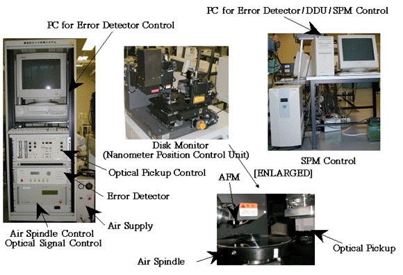
Fig.1