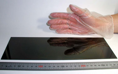
Toshiya Kumagai and Takaaki Manabe, the head and chief scientists of the Institute for Materials & Chemical Process Inorganic Solid State Chemistry Group of the National Institute of Advanced Industrial Science and Technology (AIST), have succeeded in creating the world's largest (30cm X 10cm) epitaxially-grown oxide high-temperature superconductive (YBa2Cu3O7) film.
This large-area superconductive film can apply to passive microwave devices utilizing the low-loss characteristics at microwave frequencies in the communications area, such as filters or antennas, and other devices utilizing instantaneous transition from super-conduction to normal conduction in the electric power area, such as current-limiting devices. Although severe development competitions have been carried on so far on a global basis with the focus on vapor-phase processes such as the pulsed laser deposition method, with regard to the creation of superconductive films, a problem is that vapor-phase processes are expensive and make mass production difficult. On the other hand, AIST has continued research and development on creating a large-area superconductive film using the dipping pyrolysis process under Research and development of fundamental technologies of superconducting AC power equipments (Super-ACE) project, organized by Ministry of Economy, Trade and Industry.
This method produces ceramic film by "applying and then burning" a coating solution, so that mass production can be realized at a far lower cost than that of vapor-phase processes. AIST has basic patents on creating superconductive film using this method.
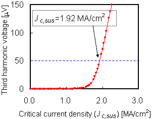
The reason it became possible at this time to create the world's largest superconductive film is that an evener and smoother ceria (CeO2) buffer layer has been successfully produced by the vacuum evaporation method over the entire surface of a sapphire substrate with a size of 30cm X 10cm, and producing the YBa2Cu3O7 film on the layer has been optimized by the dipping pyrolysis process. This superconductive film is epitaxially grown with preferentially oriented particles, and shows a very high superconductive characteristic that the maximum critical current density at liquid nitrogen temperature is 1,900,000 A/cm2. The film size is in the world's largest class, and the characteristic has achieved the goal of the Super-ACE project(FY2000-2004).
For the large-area superconductive film, a transport current measurement is to be conducted in the future in a collaborative study with the Engineering Research Association for Superconductive Generation Equipment and Materials (Super-GM), which is expected to accelerate the development of a current-limiting device of the SN transition resistor type contributing to the stabilization of electric systems.
 |
 |
|
Photograph of the created superconductive film (left) and its superconductive characteristic (right)
|