Research Outline
Further increase in efficiency and cost reduction of solar cells and modules are essential for the continuous spread and establishment of photovoltaic power generation. The photovoltaic power team maintains and operates all facilities to fabricate solar modules from crystalline silicon ingots. We are researching silicon wafers, solar cells, and solar modules. Specific research subjects are as follows:
A novel process for solar cell fabrication
We are developing a new cell fabrication process using ion implantation.
Our ion implantation technique using the stencil mask is expected to significantly reduce the number of production steps of solar cells while increasing their efficiency.
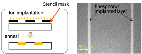 【Fig. 2】Ion implantation technique using the stencil mask.
New concept solar cell: “Heat recovery solar cell”
Conventional solar cells discard more than half of solar energy as heat. We theoretically presented a new concept of nonequilibrium solar cell, heat recovery solar cell (HERC cell). HERC cell recovers thermal energy to allow its power conversion efficiency to exceed the Shockley-Queisser limit (29%) of silicon solar cells. We are conducting experiments to realize this new concept of solar cells.
Improvement in PV module reliability
We are investigating degradation modes of PV modules by accelerated aging tests to improve the reliability of PV modules. Our modules, using the double glass structure and the wiring with conductive films, showed improved reliability in dynamic mechanical load (DML) test.
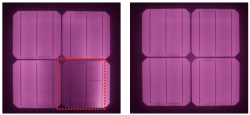 【Fig. 3】Electroluminescence images for the PV modules with a standard structure (left) and a double glass structure (right) after 16,000 cycles of DML test.
Next-generation multi-junction solar cell “smart stack technology”
The “smart stack technology” using metal nanoparticle arrays has been developed, making the interconnection of various solar cells with different materials and bandgaps possible for the first time. This provides flexibility in material choice and device design because the mismatch in lattice constants, thermal expansion coefficients, etc. can be disregarded with this technique.
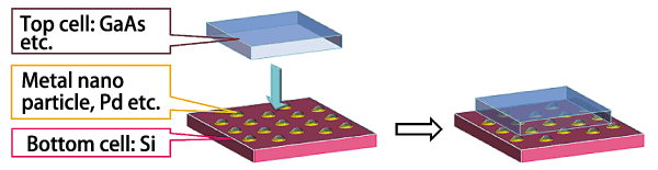 【Fig. 4】Smart stack technology
A GaAs/InP-based four-junction solar cell has achieved conversion efficiency as high as 31.6%, and a GaAs/CIGS-based three-junction solar cell has achieved conversion efficiency as high as 24.2% (joint research with the Research Center for Photovoltaics at AIST Tsukuba Center). We are working to improve and establish this technology for mass production.
The use of thin crystalline silicon as a bottom cell provides high efficiency and low-cost multi-junction cells. The team is developing crystalline silicon based smart stack cells that go beyond the theoretical efficiency limit of single-junction crystalline silicon solar cells (29%). A demonstration GaAs/Si three-junction cell with conversion efficiency of 25.1% has been successfully fabricated.
 【Fig. 5】GaAs/Si-based three-junction smart stack cell
Main Research Facilities
【Fig. 6】Electrode firing furnace
Furnace for forming contacts between the electrode and the diffusion layer as well as Al‒BSF layers.
【Fig. 7】Spin etching apparatus
Apparatus that etches a single side of the wafer by spin rotation. Only one side can be etched without a protective film.
【Fig. 8】Ion implantation equipment
Equipment that implants accelerated phosphorus or boron ions in the wafer. The diffusion profile can be precisely controlled.