Minimal Fab: Semiconductor Device Production on Demand at Low Cost
For semiconductor manufacturing, huge factories (mega fabs) made up of expensive, large-scale manufacturing equipment and cleanrooms used to be necessary. However, for low-volume production and trial manufacturing, the extremely high cost has been a problem. The solution to this problem is a minimal fab. With minimal fabs, manufacturing costs are reduced to 1/100 (to 1/1000) of the original cost, due to downsizing and standardization of manufacturing equipment.
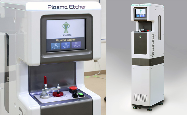
A "minimal fab" is a small-scale semiconductor factory that does not require a cleanroom. It is a production system that consists of minimal equipment, a group of small manufacturing tools, such as for wet process, exposure, film formation, etc., with a streamlined, common design. Rather than a large wafer with a diameter of 300 mm, a half-inch wafer with a diameter of 12.5 mm is employed. The standard manufacturing process is one wafer flow, and the processing in each tool is carried out in one minute.
Currently, large investments and huge factories are necessary for semiconductor manufacturing, which are possible only for a few companies even globally. Such huge factories are unsuitable for high-mix low-volume manufacturing since it requires a great deal of time and cost. However, using minimal fabs, the problem of cost and delivery time is resolved. In addition, the development and trial manufacturing of semiconductors becomes easy and simple, leading to the development of Japan's semiconductor industry as a whole. The world is now focusing on minimal fabs, which have the potential to revolutionize semiconductor production technology.