Koichi Fukuda (Senior Researcher) and co-workers of Nanoscale Characterization and Processing Research Group, the Nanoelectronics Research Institute (Director: Seigo Kanemaru) of the National Institute of Advanced Industrial Science and Technology (AIST; President: Ryoji Chubachi), have developed a circuit-characteristics analysis system that can reflect the detailed shape of a circuit pattern (lithography pattern) transferred to a large-scale integrated circuit (LSI) board.
The developed system analyzes circuit characteristics using Technology CAD (TCAD), taking into account the detailed shape of a micro-pattern predicted by lithography simulation. By using this system, the researchers have predicted the characteristics of FinFET-based static random access memory (SRAM) circuits and determined the effects of pattern shapes unique to FinFETs on circuit characteristics. This system can be used to optimize LSI fabrication processes by simulating from semiconductor fabrication processes through to circuit characteristics of device structure; it is expected to contribute to the design of next-generation LSIs. Details of this technology will be presented at Photomask Japan 2013 to be held in Yokohama, Kanagawa Prefecture, from April 16 to18, 2013.
 |
|
Analysis of the stability of a SRAM circuit from a lithography pattern |
In recent years, with advances in LSI technology, miniaturization of the transistors used in LSIs has been facing its limit. It has become serious that even the LSI patterns formed by using the latest photolithography technology deviate from their ideal shapes. There is an urgent need to develop a design method that considers manufacturability and in which the effects of these deviations on circuit performance can be determined.
Recently, to realize such a design method, a technology for building and using a database of the variations in the shapes formed during the fabrication process and a technology for correcting the photomask patterns, have entered practical use. However, there is no technology for predicting the shapes of the micro-patterns formed during the fabrication process and evaluating circuit characteristics by reflecting these shapes.
To address this issue, by combining the latest photolithography simulation technology and TCAD technology, AIST has been working to develop an analysis system for circuit characteristics reflecting the detailed shapes of lithography patterns.
Part of this research used simulation results obtained in a joint research with ASML Japan Co. Ltd. and its photolithography simulator, Tachyon. Also used was the TCAD system, HyENEXSS, that was provided through a joint research with Semiconductor Technology Academic Research Center.
If the micro-pattern of an LSI predicted by a photolithography simulator etc. is available, the developed circuit-characteristics analysis system can predict from the device structure through to the circuit characteristics of a transistor reflecting the micro-pattern by using semiconductor fabrication process simulation and semiconductor device simulation, which are TCAD technologies. First, the shape of the predicted micro-pattern is prepared in a layout format such as standard GDS-II. The system uses semiconductor fabrication process simulation to replicate the fabrication processes considering the predicted micro-pattern shape and predict the micro-structure of the multiple semiconductor devices, such as transistors, that are used in an LSI. Then, the system uses semiconductor device simulation to predict the electrical characteristics of each semiconductor device from its structure, and it uses device-circuit hybrid simulation to predict the characteristics of the circuits formed by connecting the semiconductor devices.
Figure 1 shows the photomask pattern of a FinFET-based SRAM circuit and the predicted pattern by a lithography simulator, superimposed on each other. In a micro-LSI circuit such as this, deviations occur in a formed pattern due to the distribution of the intensity of light exposure in the lithography process, even if a rectangular photomask is used.
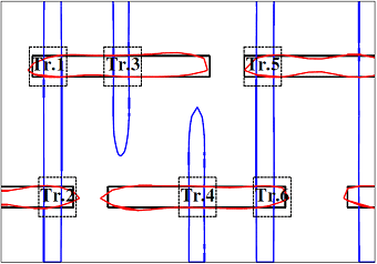 |
Figure 1 : Rectangular photomask patterns in a FinFET-based 6-transistor SRAM design and the pattern predicted by lithography simulation, superimposed on each other
Black dotted lines show the locations where transistors are formed. Black solid lines show gate patterns in the design; red solid lines show gate patterns predicted by simulation; and blue solid lines show fin patterns predicted by simulation. |
Figure 2 shows the device geometry and the impurity distribution of a transistor formed in the FinFET fabrication processes predicted by the semiconductor fabrication process simulation based on each calculated transistor pattern. The materials and shape are shown on the left, and an example of the distribution of the dopant impurities introduced by ion implantation is shown on the right. As shown in the figure, the transistors formed in the actual fabrication processes are affected by the shape of the micro-pattern and is formed into a shape different from that of the designed rectangular pattern. This affects the dopant impurity distribution, which determines the characteristics of the transistor.
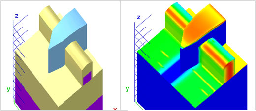 |
Figure 2 : Materials and shape (left) and an example of a dopant impurity distribution (right) of the FinFET in Tr. 1 part in Fig. 1 calculated by semiconductor fabrication process simulation
The predicted pattern by lithography simulation is taken into account. |
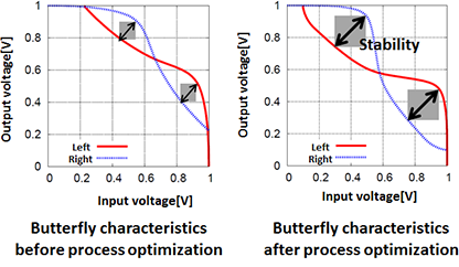
Figure 3 shows examples of the butterfly characteristics and static noise margin (SNM) characteristics curves for SRAM calculated by device-circuit hybrid simulation. Shown on the left is a characteristics curve before optimization of the fabrication conditions. The curve indicates that the yield decreases owing to the small SNM. Shown on the right is a characteristics curve after optimization of the fabrication conditions. There is a substantial improvement in SNM. As shown in the figure, the developed system allows the whole simulation of circuit characteristics, reflecting the device structure obtained from the lithography pattern. As a result, micro-pattern LSIs can be produced with higher yields by optimizing the LSI fabrication processes to suit the circuit characteristics obtained from the mask pattern.
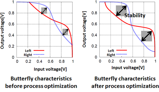 |
Figure 3 : Static noise margin (SNM) of FinFET SRAM circuits predicted by using the developed system
The arrows on the voltage-voltage characteristics curves are the SNM values, which are indexes of circuit stability. The initial SNM (left) was substantially improved (right) by optimization of the fabrication processes. |
The developed circuit analysis system will be provided to LSI developers and will accelerate the realization of LSIs using micro-devices. The system will be used as common infrastructure for the collaborative research by industry and universities into next-generation technology at the Tsukuba Innovation Arena for Nanotechnology (TIA-nano) and Super Clean Room (SCR) Industry-Academia-Government Collaborative Research Building of AIST.