Kazuma Kurihara (Senior Researcher) and Hideki Takagi (Leader), Large Scale Integration Team, the Research Center for Ubiquitous MEMS and Micro Engineering (Director: Ryutaro Maeda) of the National Institute of Advanced Industrial Science and Technology (AIST; President: Tamotsu Nomakuchi), have developed a microelectromechanical systems (MEMS) device fabrication technology that uses only printing and injection molding. This has been achieved by integrating the microfabrication technology and the MEMS design evaluation technology of AIST. A lighting device has been fabricated by combining the signal processing technology of Design Tech Co., Ltd. (President: Hatsuo Suzuki) with the developed technology.
The developed technology makes it possible to fabricate MEMS devices by using the printing technology that enables the fabrication of large-area devices without a vacuum process and the injection-molding technology that requires small capital investment and enables low production costs. MEMS devices currently produced by using semiconductor manufacturing processes can now be fabricated inexpensively and with a small capital investment. This allows the applications of MEMS devices in fields where MEMS cannot currently be used owing to high production costs and low production volumes. For example, new applications in the lighting industry can be developed by combining active variable light distribution by a MEMS mirror and LED lighting.
MEMS devices fabricated by using this technology will be presented at the Micromachine/MEMS Exhibition held at Tokyo Big Sight (Koto-ku, Tokyo) from July 11 to 13, 2012 and at AIST Open Lab held at AIST Tsukuba from October 25 to 26, 2012.
 |
|
(Figure) : MEMS mirrors for active light distribution fabricated by using only printing and injection molding (left), and examples of the resulting light distribution patterns (right) |
MEMS devices such as acceleration sensors, gyro sensors, and mirror devices for displays are currently commercially available. However, conventional MEMS fabrication techniques use the same semiconductor manufacturing systems that are used to produce large- and small-scale integrated circuits, and they require several tens of processes, including vacuum processes. MEMS fabrication therefore requires large capital investment and has high production costs that cause problems.
AIST has a test mass-production line for 8-inch-wafer MEMS and has been working on the test mass-production and development of MEMS devices in collaboration with the private sector. The present researchers are also developing a micro-molding technology that uses nanoimprinting and injection molding. They have developed large-area nanostructured anti-reflective lenses (AIST Press Release on April 23, 2007) and substrates with controlled hydrophilicity/hydrophobicity that utilize nanostructures (AIST Press Release on October 13, 2009).
The researchers have developed a technology for fabricating MEMS devices by using only printing and injection-molding processes. To do this, they have integrated fabrication and evaluation techniques obtained through the development of MEMS devices using semiconductor manufacturing processes and micro-molding technology that is low-cost and can be applied to mass production. This has led to the development of a MEMS device fabrication technology that requires reduced capital investment, can be applied to small-lot production, and has low production costs.
This R&D project was supported by the Funding Program for World-leading Innovative R&D in Science and Technology, "Research and Development of Integrated Microsystems", of the Japanese Cabinet Office.
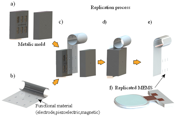
To drive a MEMS device, patterns of wiring and functional materials need to be formed onto moving microstructures. Attempts have been made to use resins for MEMS structures. However, the production cost is high because the same vacuum processes as that used in semiconductor manufacturing are used to form the metal wiring pattern. The researchers have realized the low-cost fabrication of resin MEMS structures in which the patterns of metal wiring and functional materials are formed using a low-cost printing process and transferred to the structure using an injection-molding process. Moving MEMS structures, such as springs and cantilevers, must be thin. However, it has been difficult to form thin resin structures because a molten resin begins to harden immediately after being injected into the mold. The researchers have made it possible to fill thin moving structures with a resin by improving the mold structure. Thus MEMS devices can be fabricated by using a molding process. This fabrication technique can be used to form MEMS structures inexpensively by using only a replica molding technique once the mold is created.
Figure 1 shows the MEMS fabrication processes using printing and injection molding. First, a film for transfer of the MEMS functional layer is formed (Fig. 1b). The release layer and the MEMS functional layer are printed onto the film by using a screen or gravure printer. After alignment, the printed film is put into an injection mold (Fig. 1a and 1c). After the mold is closed, a molten resin is injected into it. The resin is then cooled and solidified into the MEMS structure (Fig. 1d). In the last step, the mold is opened and the MEMS structure is separated from the film removed from the mold. The ink layers printed on the film are thus transferred to the MEMS structure (Fig. 1e and 1f).
 |
|
Figure 1 : MEMS fabrication processes by printing and injection molding |
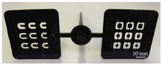
Figure 2 shows examples of MEMS devices fabricated by using the developed technology. A reflective mirror and a mirror displacement sensor are incorporated into the MEMS mirror device for lighting (Fig. 2a). A mirror ink for the reflective mirror, a conductive ink for the strain sensor, and a magnetic ink for driving the mirror are printed on the film, and then the printed ink patterns are transferred to the MEMS structure by injection molding. The MEMS mirror device for lighting did not break after more than 100 million operations driven by an external coil. A MEMS device array can be fabricated using an arrayed MEMS pattern mold (Fig. 2b).
|
(a) Molded MEMS mirror for lighting (left) and its schematic (right) |
 |
|
(b)Molded optical MEMS mirror array |
|
|
|
Figure 2 : Examples of MEMS devices fabricated by using the developed technology |
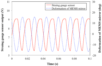
Figure 3 shows the displacement of the MEMS mirror for lighting and the output signal from the displacement sensor at different mirror angles. The displacement was directly measured with an optical measurement system. The resistance of the conductive ink changed in response to the displacement of the mirror, indicating that the displacement sensor worked properly.
 |
|
Figure 3 : Output of the displacement sensor in response to displacement of the mirror |
The MEMS device fabrication technology using printing and injection molding enables the low-cost fabrication of various MEMS devices, for example sensing devices such as acceleration sensors and gas sensors, and power generation devices, by changing the printed MEMS functional layers in accordance with the purpose. This makes it possible to provide low-cost MEMS devices in fields where MEMS devices cannot currently be used owing to the high cost of MEMS fabricated using conventional semiconductor manufacturing processes. For example, in the lighting industry, light distribution control of LED lighting is attracting attention. When MEMS mirrors are produced using semiconductor manufacturing processes, the production cost depends on the number of devices per wafer. Therefore, the production cost of large mirrors is very high, while the use of micro-mirrors requires convergence of light, making the lens optical system complex. The developed technology can be used to produce low-cost large MEMS devices (larger than several millimeters across) and therefore active light distribution control devices can be realized easily.
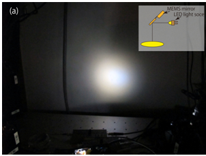
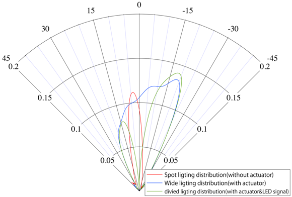
Figure 4 shows examples of the distribution of light to left and right by controlling the drive of the MEMS mirror synchronously with the timing of lighting of the LED. Active light distribution was achieved with the MEMS mirror. Figure 5 is the light distribution characteristics. The light distribution was changed between spread angles of 10° (Fig. 4a and the red line in Fig. 5) and 50° (Fig. 4b and the blue line in Fig. 5) by controlling the drive of the MEMS mirror. As shown in Fig. 4c and by the green line in Fig. 5, the light can be split by controlling the drive of the MEMS mirror synchronously with the timing of lighting of the LED. In the next step, the researchers will improve the symmetry and expand the range of the light distribution by improving the arrangement of the optical system, the signal processing, and the control circuit. Injection molding can be used easily to form three-dimensional objects of complex shape such as spheres, and the researchers expect MEMS devices to be formed on the surface of, or inside, three-dimensional objects.
 |
 |
|
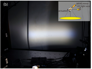
(a) The MEMS mirror is not moving. |
(b) The MEMS mirror is driven and the LED is continuously lit. |
 |
|
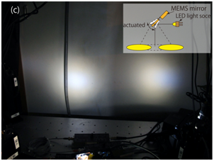
(c) The MEMS mirror is driven synchronously with the timing of lighting of the LED to achieve the split distribution of light. |
Figure 4 : Light distribution
Light from the LED is reflected by the MEMS mirror and projected onto the wall. |
 |
|
Figure 5 : Light distribution characteristics |
The injection-molding system used is commonly available in Japan. Injection-molding systems have lower market prices than semiconductor manufacturing systems and they have relatively low investment barriers. Japan is strong in the technologies for both mold-making and molding. Use of the developed technology is expected to enable non-semiconductor industries such as the plastics molding industry to begin manufacturing MEMS devices, which are products of only the semiconductor manufacturing sector so far. Entry of companies from different sectors into the MEMS manufacturing business will lead to the development of new applications of MEMS devices.
To develop applications of the developed MEMS device fabrication technology, the researchers intend to work actively with companies in a variety of industries and help to create opportunities for them to start new businesses.