- Contributes to the design of ultra-low-power, large-scale integrated circuits -
Koichi Fukuda (Researcher) and others, Collaborative Research Team Green Nanoelectronics Center (Leader: Naoki Yokoyama), the Nanoelectronics Research Institute (Director: Seigo Kanemaru) of the National Institute of Advanced Industrial Science and Technology (AIST: President: Tamotsu Nomakuchi), have developed a compact model for circuit simulation to predict the circuit behavior of tunnel field-effect transistors (tunnel FETs).
This device-operation model simulates current-voltage characteristics by predicting the electric field distribution in a tunnel FET and estimating the tunnel current. It is described in Verilog-A language and therefore can be incorporated into existing major circuit simulators. The model is expected to contribute to the design of tunnel FETs aiming at the realization of ultra-low-power circuits.
Details of this technology will be presented at the 2012 International Conference on Solid State Devices and Materials (SSDM 2012) to be held in Kyoto from September 25 to 27, 2012.
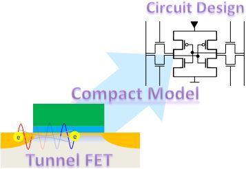 |
(Figure) : Flow to the design of a large-scale integrated circuit using low-voltage tunnel FETs
A circuit can be designed by using the device-operation model to represent the characteristics of developed devices. |
In recent years, with the wide spread of mobile information devices and the increasing sophistication of IT equipment, there has been growing concern about increasing power consumption. There has also been growing social demand for reduction in the power consumption of electronic information devices. However, reduction in the power consumption of conventional metal-oxide-semiconductor field-effect transistors (MOSFETs) is reaching its limit. Breakthrough, revolutionary low-power large-scale integrated circuits (LSIs) are required to build a low-carbon society.
In recent years, attention has been focused on tunnel FETs, which is capable of steep on/off switching at low voltage, as an alternative to the conventional MOSFETs. Use of the tunnel FETs is expected to reduce the power consumption of LSIs. Circuit simulation to determine whether new designs of LSI meet performance requirements is essential. However, it is difficult to take into account the tunnel effect in predictions of the current-voltage characteristics of tunnel FETs, and there is no tunnel FET device-operation model that can be used for circuit simulation.
Collaborative Research Team Green Nanoelectronics Center (GNC) at the Nanoelectronics Research Institute of AIST was established in April 2010 and is composed of researchers from AIST and five companies (Fujitsu Laboratories Ltd., Toshiba Corporation, Hitachi, Ltd., Renesas Electronics Corporation, and ULVAC, Inc.). Since 2011, GNC has been developing tunnel FETs with the goal of reducing the power consumption of LSIs to 1/10 to 1/100 of conventional ones. It has also been developing a tunnel FET device-operation model for the circuit simulation of LSIs.
The present research is supported by Funding Program for World-Leading Innovative R&D on Science and Technology (FIRST program) of the Japan Society for the Promotion of Science; the program has been designed by the Council for Science and Technology Policy.
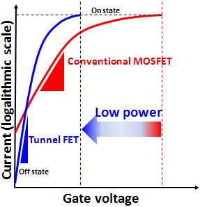
A tunnel FET is a transistor that controls on/off switching by inducing tunneling with a gate voltage, unlike the MOSFET used in conventional LSIs. Figure 1 is a schematic of a tunnel FET. The energy levels of the valence band and the conduction band of the channel are rapidly changed by controlling the gate voltage. As a result, as the energy level of the conduction band of the channel approaches that of the valence band of the source, tunneling occurs between the source and the channel, and current flows through the transistor. The tunnel FET based on this principle switches current on and off at a lower voltage than a conventional MOSFET and is capable of steep switching. As shown in Fig. 2, if the switching is steep, the tunnel FET can operate at a lower voltage than a conventional MOSFET. As a result, an LSI using tunnel FETs can also operate at a lower voltage.
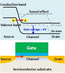 |
Figure 1 : Structure and device principle of the tunnel FET
The dotted gray lines indicate the off state. |
 |
|
Figure 2 : Steep switching characteristics of the tunnel FET |
The developed compact model for tunnel FETs can calculate the tunnel current generated in the FET from the terminal voltages of the source, drain, and gate. First, the model predicts the electric field distribution at the location in the tunnel FET where the tunnel current is generated. The tunnel distance can be obtained from the electric field distribution, allowing estimation of the amount of the generated tunnel current. Because the model can be used to predict the electrical characteristics of individual devices, a circuit simulator with the model can quickly predict the performance of a circuit with multiple devices connected to it. This makes it possible to design an LSI circuit that uses tunnel FETs. In addition, the model is described in Verilog-A language and therefore can be incorporated into various circuit simulators.
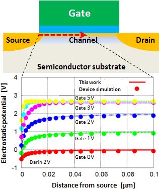
Because a circuit simulation deals with multiple devices simultaneously, the model is expressed by analytical equations that can be calculated instantly. The validity of this model was evaluated by comparison with numerical simulations, including a numerical analysis method that divides a device structure into a group of small regions and solves equations (the finite element method). Figure 3 compares the electrostatic potential distribution predicted by the device-operation model and the results of a numerical simulation with various terminal voltages. The electrostatic potential distributions in the cross-section of the tunnel FET along the gate dielectric layer are shown. The electrostatic potential distribution predicted by this model agrees well the numerical simulation, which takes 10 minutes to 1 hour for the calculation of one device. The tunnel distance can be obtained from the electrostatic potential distribution, making it possible to quickly and accurately calculate the amount of the tunnel current.
 |
|
Figure 3 : Comparison between the electrostatic potential distribution predicted by the compact model and numerical simulation results Electrostatic potential distributions in the direction of the arrow at the interface for different gate voltages (Vgs) are shown. |
Figure 4 compares the current–voltage characteristics of a tunnel FET obtained by using the device-operation model and measured values. The example in the figure is for the tunnel FET that switches on when the gate voltage is negative. It shows that this model can accurately simulate the operating characteristics of the tunnel FET. When incorporated into a circuit simulator, the model can simulate an LSI that uses tunnel FETs. Use of the model is expected to help in the circuit design and power-consumption-reduction of LSIs.
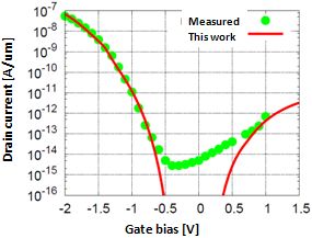 |
Figure 4 : Comparison between measured values and results of a simulation of current-voltage characteristics of the tunnel FET
Note: The difference in values near a gate voltage of 0 V is due to the leakage current through the gate dielectric layer observed in the measurement and is not specific to tunnel FETs. It can be suppressed by device design and therefore was ignored in the calculation. |
The researchers intend to provide the developed compact model to researchers of low-power circuits and to thereby accelerate the development of low-power LSIs that use tunnel FETs.