- Development of a high-performance micro-optical converter to scale transmitted signal light -
Masatoshi Tokushima (Associate Manager) and Akio Kamei (Officer), Integrated Device Processing Office, Innovation Center for Advanced Nanodevices (Director: Hiroyuki Akinaga) of the National Institute of Advanced Industrial Science and Technology (AIST; President: Tamotsu Nomakuchi) and Tsuyoshi Horikawa (Senior Researcher), Nanoelectronics Research Institute (Director: Seigo Kanemaru) of AIST, have developed an advanced technique for direct optical coupling of a silicon photonics-based optical integrated circuit (optical IC) to optical fibers, in collaboration with NEC Corporation (President: Nobuhiro Endo).
The technique enables highly efficient input and output of the optical signal from the optical fibers to and from the optical waveguide in the optical IC. Conventional direct coupling techniques suffer a significant optical signal loss due to the optical waveguide being much narrower than the optical fiber, and to the difference in the refractive index between the waveguide and the fiber. The researchers have developed a high-efficiency optical coupling technique that can reduce the optical loss to less than 1 dB per end face using an optical converter of a new structure that can change both the diameter of the signal light passing through the optical waveguide and the refractive index at the coupling end face. This technique allows low-loss optical coupling of an optical IC to standard optical fibers and an easy assembly process for optical coupling. Thus, it is expected to contribute to a reduction in the cost of a multi-channel optical IC.
Details of this technique will be published online in Applied Physics Express on February 6, 2012 (10 am, JST).
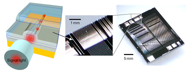 |
Optical converter to reduce the diameter of the signal light from the optical fiber (left),
and optical IC with multiple optical converters (middle and right) |
With increasing demands for processing large volumes of data, such as video data, on communication equipment including PCs and mobile phones, the load on optical fiber communication networks that transmit such data is increasing. The density of the communication networks has been increased to transmit a large volume of data at a higher speed. As a result, the number of devices to control optical signals (node devices) has rapidly increased, causing concerns about increasing power consumption. To address this issue, research on technology to replace node devices with very-low-power consumption optical ICs is being actively conducted. The volume of data transmitted through the optical fiber communication networks is expected to continue to increase. A multi-channel optical coupling technique for easy coupling of a number of optical fibers is needed to manage the increasing data traffic using optical ICs. However, the techniques using conventional optical converters do not allow highly efficient and easy multi-channel optical coupling by directly connecting to standard optical fibers.
In recent years, silicon photonics, a technology for integrating silicon optical circuits on a silicon chip, has been attracting attention. AIST is conducting research and development of silicon photonics-based optical ICs for communication, and has a world-class technology for a low-loss optical waveguide in the optical ICs.
To realize an optical IC, various optical elements to process optical signals in the optical IC must be developed. Also important is the development of an optical converter for input and output of the optical signal from the optical fiber to and from the optical IC. Unlike an electric signal, an optical signal is not properly transmitted by simply connecting to an optical fiber. The optical waveguide in the optical IC is much narrower than the optical fiber and requires the IC to have an optical converter that can change the diameter of the light beam. Conventional optical converters do not have the scaling ability sufficient for direct coupling to standard optical fibers. Therefore, it is necessary to use a lens or provide an optical converter on the optical fiber side. This limits the number of channels coupled to optical fibers and requires many assembly steps.
To solve this problem, AIST has been working to develop an advanced optical coupling technique for easy and efficient assembly which allows optical coupling by simply butting an optical fiber to the optical waveguide in the optical IC.
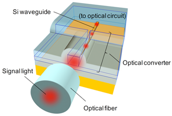
The optical circuit of a silicon photonics-based optical IC consists of silicon optical waveguides. The cross section of the light beam passing through the waveguides is usually around or less than 1 µm square. On the other hand, the diameter of the light beam passing through a standard optical fiber for communication is 10 µm. Thus, there is a 10- to 100-fold difference in beam diameter. For low-loss optical coupling by simply butting an optical fiber to the optical waveguide, an optical converter that can scale the beam diameter at this magnification needs to be provided in the optical IC. Also, it is important to control the reflection of the light beam at the coupling interface due to the difference in the refractive index between the fiber and the waveguide by making the refractive index at the coupling end face on the waveguide side equal to that of the fiber. The researchers have developed an optical converter that meets these two requirements and can scale the diameter of the signal light, which realizes direct coupling of the optical IC to a standard optical fiber. The optical converter is placed at the edge of the optical IC chip and has a silica rib optical waveguide with transversely increasing thickness toward the coupling end face overlaid on the end of a tapered silicon optical waveguide. In other words, it has a dual tapered structure with double cores of two different materials tapered in opposite directions to each other.
 |
|
Figure 1 : Optical converter that can scale the beam diameter of the optical signal between the silicon optical waveguide and the optical fiber |
Figure 1 shows the internal structure of the optical converter and how the waveguide is optically coupled to the optical fiber. In this converter, both the tapered silicon waveguide and the tapered silica waveguide, composing the dual tapered structure, have the ability to scale the diameter of the light beam; and the beam diameter can be scaled at high magnification, which has been difficult with a single tapered structure. Even though the optical waveguide in the optical IC is silicon with a high refractive index (3.5), the reflection at the coupling interface with the optical fiber can be sufficiently reduced because the material of the coupling end face changes to silica having the same refractive index (1.5) as the optical fiber. Due to these effects, optical coupling to a standard optical fiber can be achieved with only a small optical loss of less than 1 dB per end face.
The researchers have worked on the improvement of fabrication process of the optical converter as well as its structural design. A gentle slope can be created by forming a photoresist pattern projecting out at the top on a silicon substrate and etching the surface using the photoresist as a mask. A sufficiently gentle slope of silicon at an angle of less than 1° can be created using the photoresist pattern that is a few hundred times as thick as an ordinary one, while maintaining mass productivity.
 |
|
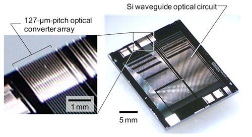
Figure 2 : Optical IC (right) containing the fabricated optical converter array (left) |
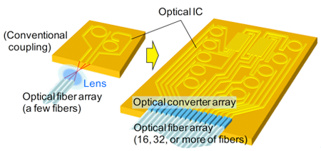
Figure 2 is an example of an optical IC containing the optical converter array. The optical converter array consists of equally spaced optical converters allowing multi-channel optical input/output to and from the optical IC. An optical fiber array is coupled to the optical converter array. Optical fiber arrays of several to several ten equally spaced (at 250 or 127 µm) standard optical fibers are commercially available. If an optical converter array, which allows direct optical coupling to an optical fiber array, is available, multi-channel optical input/output to and from the optical IC can be easily achieved. As shown in Fig. 3, the developed optical coupling technique allows highly efficient optical coupling by simply connecting the optical fiber array directly to the optical converter array, and is expected to promote multi-channel optical ICs.
 |
|
Figure 3 : Multi-channel optical IC easily achieved through combination of the optical converter array and the optical fiber array |
The developed technique can be applied to optical ICs for relatively short-distance optical interconnection as well as those for long-distance communication. The researchers will make this technique available for the development of various optical ICs through new projects and joint research projects undertaken at AIST; and thereby disseminate the technique as a standard optical coupling technique for multi-channel optical ICs that support the society in which a large volume of information is processed.