-High scanning speeds of more than 25 kHz as well as large scanning angles such as 100° or greater were achieved –
Jaehyuk Park (Research Scientist), Integration Process Technology Group, and Jun Akedo (Principal Research Scientist and Leader of the group), the Advanced Manufacturing Research Institute (Director: Norimitsu Murayama) of the National Institute of Advanced Industrial Science and Technology (AIST; President: Tamotsu Nomakuchi), developed a metal-based high-speed optical scanning devices (optical scanners) for projection displays etc. The devices can achieve higher performance and fabricate at lower cost, compared with conventional optical MEMS scanning devices.
The developed optical scanning devices employed an AIST-original MEMS driving method, Lamb-wave-resonance piezoelectric driving method. It achieved large optical scanning angles of 100° or greater at high scanning speeds (25 kHz or higher) and low driving voltages (20 V or less), those are required to be used in practical projection displays. Owing to the use of a metal-based structure, manufacturing cost will be reduced to one-tenth of the existing manufacturing cost. The device also passed a continuous durability test for more than thirty thousand hours, and the fluctuations in the scan time for twenty thousand scans were less than the order of nanoseconds.
This metal-based high-speed optical scanning device will be exhibited with its application devices such as display devices at nano tech 2010 International Nanotechnology Exhibition & Conference held on February 17–19, 2010, at Tokyo Big Sight.
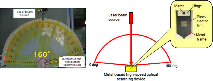 |
The metal-based high-speed optical scanning device employing the Lamb-wave-resonance piezoelectric driving method.
A laser beam from the upper light source are reflected by the optical scanning device and projected onto a wide-angle area. |
Projection displays such as portable projectors and laser displays, which use laser light sources, are expected to possess not only high color reproduction capabilities (wide color range) of video display equipment but also power-consumption reduction capabilities. In recent years, high-performance high-speed optical scanning devices that can be manufactured at low costs attract attention as the key component to realize the capabilities.
An optical scanning device comprises a reflection mirror for laser beam scanning and a driving part. The mirror scanning principle involves torsional driving method, that is, torsion bars (flexible hinges) that support the reflection mirror are twisted, and the scanning torsion angle of the mirror is increased by a resonance phenomenon caused by the vibration of the driving part.
Optical scanning devices can be applied not only to portable projectors, large-screen laser displays, head-mounted displays, and head-up displays but also to various kinds of sensors and laser printers. There has been rapid advancement in the development of small optical scanning modules with a size of several square centimeters in which these optical devices are used (Fig. 1).
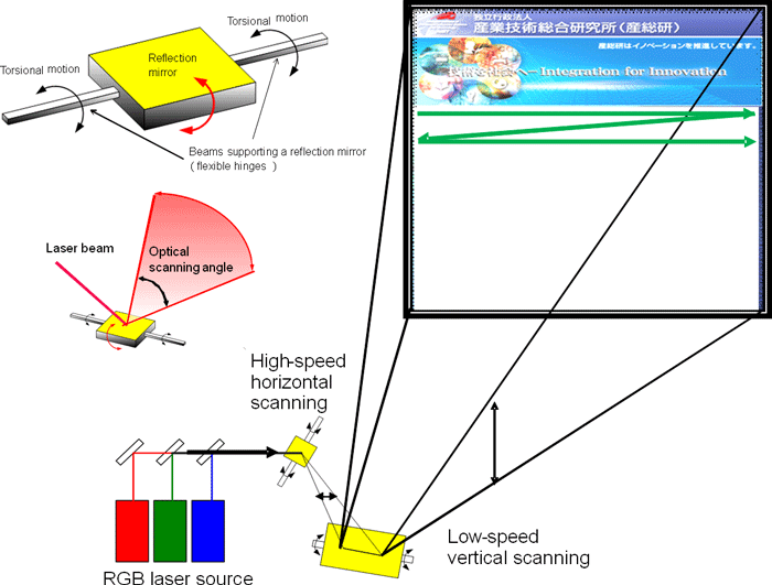 |
Figure 1 Structure of an optical scanning device and the operating principle of projectors using optical scanning devices.
Similar to a cathode-ray tube (CRT) in a TV, a picture is constructed by the combination of high-speed horizontal laser scanning and low-speed vertical laser scanning. |
Optical scanning devices require high horizontal scanning speeds to realize high-quality projection displays. For realization of slim large-screen displays, the scanning devices require a large scanning angle. However, since a trade-off exists between the scanning speed (resonance frequency) and scanning angle in conventional optical scanning devices, optical scanning devices simultaneously with scanning speeds of 25 kHz or higher and optical scanning angles greater than 60° have not been realized.
AIST has carried out researches on the formation of piezoelectric films using the AIST-original coating technology, aerosol deposition (AD) and device application, and has promoted the development of optical scanning devices using silicon-based micro-electro-mechanical systems (MEMS) in collaboration with companies.
AIST also reviewed the driving principle of optical scanning devices, devised the novel Lamb-wave-resonance driving method, and metal-based structure, and published the possibility of the improvement in performance and reduction in costs of these devices (NIKKEI MICRODEVICES, April 2006). With the aim of practical use of such optical scanning devices, we have since developed the devices with high performance, high reliability, and high durability, which meet market needs, on the basis of design optimization and a search for metallic materials. Thus, we succeeded in drastic improvement in the durability and performance, such as the extensive improvement in the scanning angle and huge reduction in the driving voltage, and actualized a device having practical-level performance.
AIST has been conducting this research jointly with Micro Precision Co. & Ltd., NEC TOKIN Corporation, and Fine Rubber Laboratories Co., Ltd. under a project commissioned by the New Energy and Industrial Technology Development Organization (NEDO); the project is named as "Research and Development of Nanodevices for Practical Utilization of Nanotechnology: Development of high-stable optical scanners for laser TV using high-performance AD piezoelectric films and nanotube-filled rubbers." AIST has also collaborated with Shinano Kenshi Co., Ltd. under the Product performance evaluation project for small and medium enterprises commissioned by the Ministry of Economy, Trade and Industry, named as "Commercialization development of MEMS optical scanner units for laser printers."
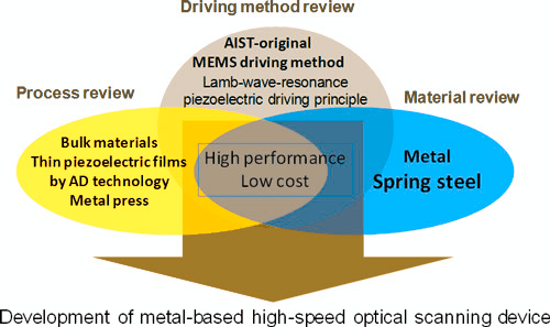
The development was carried out by reviewing the driving principle of optical scanning devices for achieving high performance and stability; this resulted in the establishment of the practically applicable piezoelectric driving principle based on the resonance of Lamb waves. To validate the effectiveness of this principle, we developed a novel optical device, a "metal-based high-speed optical scanning device," based on MEMS by changing the material of the main part of the device from single-crystal silicon to a metal, spring steel, for reducing cost and increasing durability (Fig. 2).
 |
|
Figure 2 Development flow |
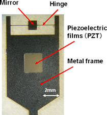
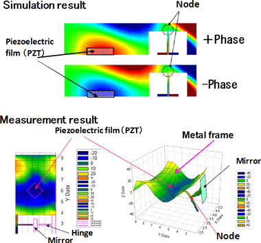
To implement the Lamb-wave-resonance piezoelectric driving principle, plate waves (Lamb waves) were generated at the device frame that was composed of a metal by employing the bending vibration mode (d31) of a piezoelectric film. By optimizing the size and location of the piezoelectric film and the shape and supporting structure of the frame, nodes (points where the wave amplitude is zero) of the plate waves are generated at the positions close to the base of the hinges that support the mirror, and torsional vibration is efficiently induced at the hinges. This novel operation principle allows the generation of torsional resonance with extremely high driving efficiency (Fig. 4) by a Lamb-wave-resonance structure where the torsional resonance system including a mirror and the driving source such as a piezoelectric film are located at remote places (Fig. 3). Thus, using this principle, the torsional resonance structure at the hinges and the frame was dramatically simplified in comparison to that obtained using conventional MEMS driving methods, and highly precise torsional vibration was achieved. Since the generated energy can be increased by widening the area of the driving source, we can make the scan of a large sized mirror at high resonance frequency with a large scanning angle. Although the piezoelectric film, which is a driving source, can be prepared by sticking a thin plate of bulk material, the direct formation of a piezoelectric film on the metallic device frame using the AD technique without adhesives has advantages including increased product yields, improved thermal properties, and reduced driving voltage.
 |
|
Figure 3 Structure of the metal-based optical scanning device |
 |
|
Figure 4 Lamb-wave-resonance piezoelectric driving principle of the metal-based optical scanning device |
Most conventional resonance-type optical MEMS scanning devices reported are applications of silicon-based MEMS. Because silicon-based MEMS are composed of single-crystal silicon wafers, and are processed using precise micro processing technology, high durability is expected even if they are used in the resonance state. Moreover, variation of the resonance frequencies among mass produced devices is considered to be suppressed. However, when silicon-based devices are actually applied to car-mounted or mobile products, they often break owing to sudden external shocks; this is because of the brittleness of silicon, and this lack of reliability is a problem. Of course, this problem may be resolved by improving the device packaging. However, since an angular aperture with high light-gathering power is determined by the mirror size, it is inevitable that for one-mirror optical scanning devices used in projectors the mirror area will be 1 mm2 or larger; this enables generation of laser beams that have high-density light-gathering power. Unlike digital light processing (DLP) projectors, the mirror size of which is 10 μm, the mirror itself has a considerable weight, and therefore, the problem of reliability against shocks may not be resolved completely. In addition, since the size of such optical scanning devices exceeds 5 mm2, relatively small number of devices can be manufactured from one silicon wafer, and hence, the production cost rises.
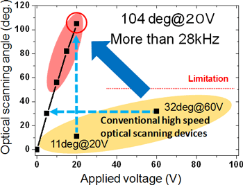
On the contrary, we used an inexpensive, highly strong, highly elastic metallic spring material, which is used in automobile parts, and optimized the design of the device using the Lamb-wave-resonance piezoelectric driving principle to improve its efficiency. Thus, even for a mirror size of 1 mm2 or larger, which is the mirror size in most optical scanning devices, we succeeded in developing the world's first optical scanning device that can simultaneously achieve high scanning speed (28 kHz) and a large optical scanning angle (104°).
The developed optical scanning device has a 100° scanning angle at a driving voltage of 20 V, which is 5–10 times larger than the scanning angle of conventional piezoelectric-driven optical scanning devices. This implies that the driving voltage required to obtain the same scanning angle is reduced to one-fifth to one-tenth and the power consumption is less than 100 mW; this opens up the possibility of the application of this device to components of mobile products, which require low driving voltage and low power consumption (Fig. 5).
 |
|
Figure 5 Relationship between driving voltage and scan angle of the developed metal-based high-speed optical scanning device |
 |
|
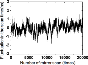
Figure 6 Mirror scanning accuracy of the metal-based optical scanning device based on the Lamb-wave-resonance piezoelectric driving principle |
With respect to the accuracy of the mirror scanning, the fluctuation in the scan time (scan period) was the order of nanoseconds for twenty thousand scans at a scanning speed of 28 kHz and an optical scanning angle of 90° in an atmosphere without electrical control (Fig. 6). That scanning accuracy is adequate for practical projection displays, and a scanning accuracy equal to or less than 3 ns, for example, can be applied to high-resolution displays such as high-definition TVs. Moreover, the developed metal-based optical scanning device passed a continuous durability test performed for more than thirty thousand hours (the test is still in progress). Until now, the use of metallic materials as structural materials has been regarded as a problem because of metal fatigue. The result obtained using our device is a new finding and is overturning long-held beliefs; our device has practical durability and can be applied to consumer products.
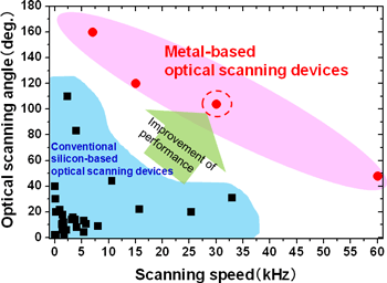
The developed devices simultaneously achieved high scanning speeds and large scanning angles, unlike conventional silicon-based optical scanning devices (Fig. 7). With respect to the size of the optical scanning device, the devices can employ mirrors ranging from several square millimeters to several square centimeters; a prototype of a two-dimensional optical scanning device has been developed. Thus, a wide range of applications can be expected. With respect to the production cost, since the unit price of the metallic spring material is roughly one-hundredth that of silicon material, and the production of the device does not need expensive production infrastructure such as clean rooms, the device would be competitively priced.
 |
|
Figure 7 Performance comparison between the metal-based optical scanning device and the conventional optical scanning devices based on silicon-based MEMS |
With the aim of exploring practical and novel applications of the developed optical scanning devices, we will vigorously promote mass production of these devices in cooperation with companies. The devices will be exhibited with their application devices such as display devices and we will perform demonstrations at the NEDO booth and AIST booth at nano tech 2010 International Nanotechnology Exhibition & Conference, held on February 17–19, 2010, at Tokyo Big Sight.