- A step toward ideally efficient semiconductor optical devices
such as light-emitting diodes -
XueLun Wang (Senior Research Scientist), the Near Field Nano Engineering Group (Leader: Takashi Tokizaki), the Nanotechnology Research Institute (Director: Nobutsugu Minami) of the National Institute of Advanced Industrial Science and Technology (AIST) (President: Hiroyuki Yoshikawa) and Mutsuo Ogura (Senior Research Scientist), the Nanotechnology Research Institute, have jointly discovered the phenomenon that more than 50% of the spontaneous emission light generated in semiconductors with microscopic V-grooves is emitted into the air, and have succeeded in explaining the mechanism involved in cooperation with a group in the Paris Institute of Nanosciences, the National Center of Scientific Research (CNRS).
Strong total internal reflection normally occurs at the interface between the semiconductor and the air because the refractive index of a semiconductor material is usually much greater than that of air. This makes it very difficult to efficiently extract spontaneous emission generated in a semiconductor material into the air. For example, in the case of semiconductor light-emitting materials formed on a flat substrate, one can only extract a few percent of the total emission generated. This is a serious roadblock to improving the efficiency of various semiconductor optical devices, such as LEDs.
In this study, semiconductor light-emitting materials are formed on substrates with microscopic V-grooves. By controlling the grooves shape, more than 50% of light generated is successfully extracted to air. When the light produced in the semiconductor material is totally reflected at the semiconductor-air interface, evanescent waves are generated. Due to the V-shaped surface structure of the material, evanescent waves originated from different crystal surfaces interfere with each other, and are transformed into light propagating in air with an efficiency of greater than 50%. This phenomenon will find applications in various types of semiconductor optical devices, especially LED, a promising device for future energy-efficient lighting and display applications.
The result of the study will be published in the electronic version of Applied Physics Letters on March 2, 2009.
 |
|
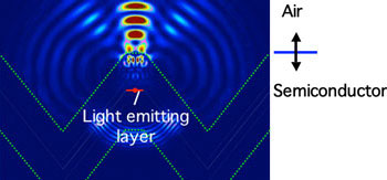
Simulation results showing the efficient extraction of light genertaed in the light-emitting layer to air through the small top flat parts between the V-grooves.
|
High-efficiency LEDs using compound semiconductors are attracting a great attention as prospective energy-saving light sources for lighting and display applications. Research and development are being pushed ahead worldwide toward widespread replacement of the conventional light bulbs and fluorescent lamps with this new light source. It is estimated that widespread utilization of LED lighting could reduce the global electricity consumption by 10%.
To improve the energy-conversion efficiency of LEDs, it is crucial to extract, as efficiently as possible, the light generated in semiconductors to air. However, it is very difficult to efficiently extract light from semiconductors to air because light tends to remain inside semiconductors owing to the existence of strong total internal reflection at the semiconductor-air interface. Although various light-extraction techniques have been proposed, we still have serious problems in efficiency and production cost. Thus, development of high-efficiency, low-cost light-extraction techniques is critically required for LED lighting to be generally accepted.
At AIST, substantial research efforts have been devoted to date to the formation of semiconductor nanostructures on substrates processed into various types of special shapes, to the investigation of optical characteristics of nanostructures such formed, and to the realization of optical devices utilizing these nanostructures. The light emission mechanism is studied in cooperation with a group in the Paris Institute of Nanosciences, the National Center of Scientific Research (CNRS).
Part of this study was supported by "Development of Ultrahigh-Efficiency Compound-Semiconductor Quantum-Wire Light-Emitting Diodes," 2007 Grant-in-Aid for Scientific Research, Scientific Research B, the Japan Society for the Promotion of Science.
It is well known that a special kind of light called "evanescent wave" appears locally on the reflecting surface when total internal reflection occurs on a material surface. This evanescent wave, after moving along the surface for a distance shorter than the emission wavelength, quickly turns back into the material, and cannot escape into the air. It is found in this study that, if nanostructured semiconductor light-emitting materials are formed on substrates with microscopic V-grooves, evanescent waves originated from two different crystal facets interfere with each other, and are transformed into light propagating in air with a very high efficiency.
As illustrated in Fig. 1, the sample used in this study is a GaAs/AlGaAs nanostructure formed on a substrate (GaAs) with microscopic V-grooves by using Metal-Organic Chemical Vapor Deposition (MOCVD). The optical characteristics of the GaAs quantum well light-emitting layer (the red parts in Fig. 1) formed under the flat portion between V-grooves are evaluated by means of photoluminescence measurement. It is very surprising to find that the light emission intensity of the quantum well grows steeply as the width of the flat portion W is reduced below 1 µm (Fig. 2). Quantitative analysis of the photoluminescence data of Fig. 2 shows that more than 50% of the light generated in the quantum well layer of the sample with a 0.5-µm wide flat part is extracted into the air. This is an extraction efficiency of about 20 times greater than that reported so far for semiconductor light-emitting materials formed on flat substrates.
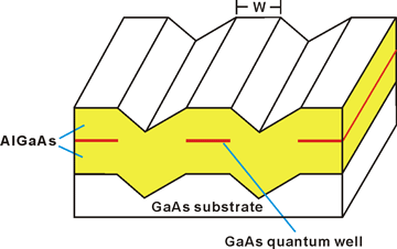
Fig. 1 Schematic of the sample used in this study.
|
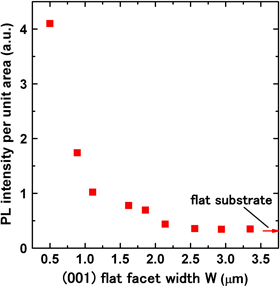
Fig. 2 Dependence of light emission intensity of quantum wells (per unit area) formed on the flat surface portion of the V-grooved substrate on the lateral width of the flat portion.
|
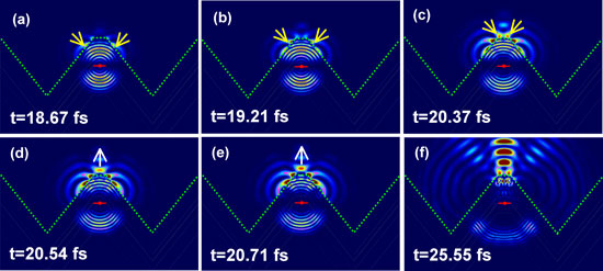
The mechanism of the increase of light emission intensity is studied by theoretical analyses and measurements of spatial distribution of light intensity. Shown in Fig. 3 is a series of simulated images demonstrating the time-dependent propagation of the light generated in the quantum well. As shown in this figure, as the light generated in the quantum well reaches the sample-air interface (green dotted lines in the figure), two evanescent waves (yellow arrows in the figure) are generated symmetrically on the two sidewall surfaces by total internal reflection. These two evanescent waves move along the sidewall surface towards the narrow top flat surface where they interfere with each other, and are efficiently transformed into light propagating in air (white arrows).
 |
|
Fig. 3 Simulation results showing the process in which evanescent wave is transformed by interference into light propagating in air (fs = femto-second).
|
The structure of semiconductor light-emitting materials will be optimized to further improve light extraction efficiency, and high-efficiency semiconductor LEDs will be developed based on this new technology.