Akiyoshi Chayahara (Team Leader) and Yoshiaki Mokuno (Senior Research Scientist) of Diamond Wafer Team, the Diamond Research Center (Director: Naoji Fujimori) of the National Institute of Advanced Industrial Science and Technology (President: Hiroyuki Yoshikawa) (hereinafter referred to as AIST) have developed a technology for the mass production of single crystalline diamond wafers.
Diamonds have excellent properties, such as high hardness, high thermal conductivity, high light-transmittance in wide wavelength region, wide band gap, and excellent stability against chemicals. So, diamonds are expected to be applied in a variety of products, such as semiconductor devices, electron-emission devices, and biosensors, as well as in tools and optical components. The applications of diamond in electronics have received particular attention because the performance of diamond-based devices is expected to surpass that of silicon or silicon carbide devices. When diamonds are used in electronic devices, it is essential to establish techniques for mass production of single crystalline wafers.
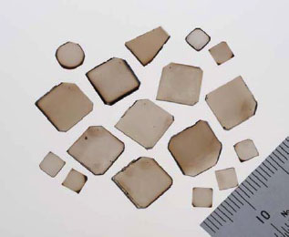
AIST has developed a technology for the mass production of large-area single crystalline diamonds by combining repetitive overgrowth from vapor-phase while changing the growth surface, with a technique for separating the newly grown diamonds from the seed diamonds with minimal loss of the seed crystals. (Photograph 1). The results of this research will be presented at the international conference on "New Diamond and Nano Carbons (NDNS 2007)" to be held at the Senri Life Science Center on May 28-31, 2007 (Shin-senrihigashimachi, Toyonaka, Osaka).
 |
|
Photo.1
|
Because of their useful properties, such as high hardness, good thermal conductivity, high light transmittance in wide wavelength region, and excellent stability against chemicals, diamonds have wide range of applications in various types of device. In particular, diamonds are expected to be applied to semiconductor devices. For this purpose, single crystalline diamond wafers that utilize the excellent properties of diamond are required. In conventional manufacturing processes, large single crystals of diamond are sliced into plate diamonds, and because of the complicated processing involved and the large amounts of processing loss, it has not been feasible to use diamond in electronic devices. A technology for the mass production of large-area single crystalline diamond wafers is therefore highly desirable.
Since 2003, the Diamond Research Center, AIST has been engaged in research on the synthesis of large single crystals of diamond by using the microwave-plasma chemical vapor deposition (CVD) method, and has succeeded in synthesizing a 1-carat single crystalline diamond.
By advancing this research, the center found that it is possible to suppress the growth of abnormal crystals that have different orientations by precise control of the surface temperature (at around 1200°C) and the amount of nitrogen in the reaction gas.
In addition, rapid synthesis at 50µm/h was possible, which is five times faster than the conventional method, and was achieved by optimizing the growth conditions of the diamond crystals. The technique has been successfully developed as the "Direct Wafer Making Technology" in which seed crystals and the diamonds grown on them can be separated with minimal processing losses, opening up the possibility of mass production of large-area single crystals of diamond.
Diamonds can be produced either by treating carbon at high temperatures and high pressures in a special furnace or by the plasma CVD. AIST has been developing a technology for producing diamonds by using the nitrogen-added microwave-plasma CVD method.
As shown in Figure 1, the AIST production method is characterized by the continuous growth on the (100) surface. First, a rod-like diamond was grown on the (100) surface of a seed crystal. Next, a side surface, for example the (010) surface, is polished, and diamond crystal was grown on the surface. The subsequent crystal growth on the (100) surface will enlarge the crystal step by step.
Photograph 2 shows a large diamond, weighing 6.6 carats, produced by using this method.
Such large single crystals of diamond can be sliced by a laser to produce diamond wafers, but this is not a practical method because it involves many processes and entails considerable and unavoidable losses of material.
In our newly developed wafer-making technology named as the "Direct Wafer-Making Technology", a defected layer is introduced into the single crystalline seed diamond by the injection of ions immediately beneath its surface before the crystal growth. Following the growth of the diamond, the defected layer transforms into a graphite structure that can be removed by electrochemical etching. This "Direct Wafer-Making Technology" entails the loss of only a very small amount of the seed crystal (1µm or less) when it is cut off. The method therefore permits reuse of the seed crystal many times. The detached wafer can also be used as a seed crystal (see Photograph 2).
Although several research institutions have conducted research on this kind of separation method, they have only succeeded in producing small-sized diamonds measuring 3 to 4mm square at the maximum. AIST has successfully produced large-area diamond wafers measuring 10mm square (10 times the area of the previously synthesized diamond plates).
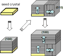
Fig.1
|
|
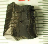
Photo.2
|
A wafer measuring more than one inch (2.54cm) is needed to open up the possibility of applying diamonds in commercial semiconductor devices. The maximum size of the wafer that we produced was 10mm square, because of limitations imposed by the CVD equipment. We will continue to improve the quality of crystals by introducing in situ observation technology while improving the plasma generator to produce uniform and large-area diamond wafers.
We wish to extend the application of diamond in the field of electronics by developing these technologies.