- Stimulating the development of next-generation high-speed routers and servers for the optical broadband age -
The Nanoelectronics Research Institute (Director: Toshimi Wada) of the National Institute of Advanced Industrial Science and Technology (AIST; President, Hiroyuki Yoshikawa) has established the Opto-Electronic System Integration (SI) Collaborative Research Team (Director: Masahiro Aoyagi; participating enterprises: NTT Advanced Technology Corporation, Sumitomo Electric Industries, Ltd., NEC Corporation, NGK Spark Plug Co., Ltd., Hitachi Chemical Co., Ltd., Hirose Electric Co., Ltd., Mitsui Chemicals Inc., Ricoh Co. Ltd., and Ibiden Co., Ltd. Our research team has successfully developed an optical backplane with high transmission capacity of 3 tera-bit per second (data corresponding to more than 70 DVDs can be transmitted within 1 second) for application to routers and servers. This capacity is five times higher than the current electric backplane in conformity with the ATCA (Advanced Telecommunications Computing Architecture) Standard decided in January 2003. We have developed a new small diameter high Δ optical fiber with a data transmission capacity exceeding 10 giga-bits per second, and a low cost, easy to assemble optical-electric conversion module for interconnections, and have succeeded, for the first time, in developing a high density optical connector to be integrated as an optical backplane in accordance with the packaging in conformity with the ATCA Standard.
Thanks to this optical backplane technology, it is possible to substantially increase the signal transmission and information processing capacity of the router and the server used for the optical broadband networks, opening new roads for practical applications in the fields of medicine and education, where ultra high definition image transmission is indispensable.
These research results were presented at the session on the Optical Electronics and Optical Interconnections of the 2005 IEICE Society Conference from September 20 to 23, 2005 held at Hokkaido University in Sapporo.
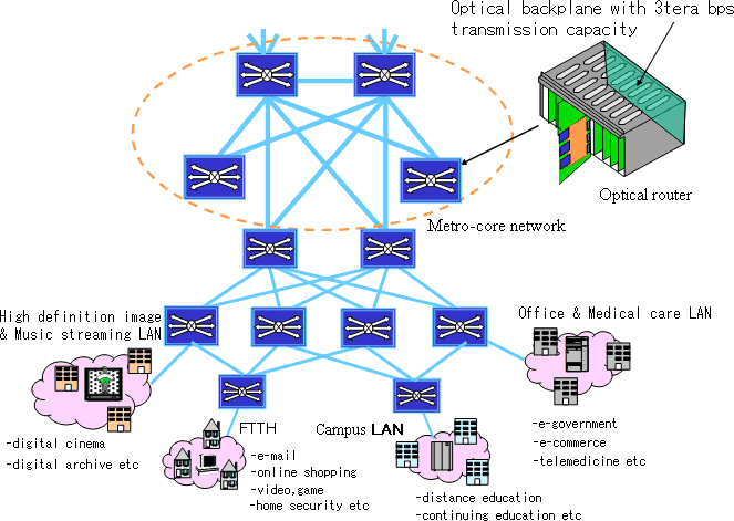
The rapid spread of the Internet has rapidly intensified the demand for an increase in the information transmission capacity of broadband networks. Conventional electric transmission circuits have almost reached the limit of transmission capacity as trunk line networks as well as communication lines to households advance quickly. To cope with this situation, the development of ultra-high speed information transmission equipment, compatible with these broadband networks, is required (Figure 1). Networks with optical cable are currently in use for this kind of information transmission service, but due to the operating speed restrictions of network connecting devices such as routers and of servers, it is becoming difficult to attain a satisfactory level of service. Because these speed restrictions are mainly due to the high frequency transmission loss of electric signal transmission in the device, if optical transmission technology with an extremely small transmission loss is used in the backplane connecting various optoelectronic components in the router and server devices, it may be possible to overcome this limitation and to achieve a drastic improvement of the capabilities of the information transmission equipment. To this end, many domestic and international corporations, including the Daimler Chrysler Corporation, are engaged in the development of the optical backplane. However, due to the strong straight guiding characteristic of light, it has been difficult to introduce the three dimensional optical wiring of the optical backplane inside the extremely narrow space of the device.
At the AIST we are promoting the development of measurement evaluation and packaging technology for ultra-high speed electric signals. From FY 2004, we have integrated these technologies with optical packaging technologies, and have carried out research and development of an optical backplane for next-generation ultra-high speed communication devices. For the research and development, AIST has concluded a collaborative research contract with 9 private corporations, each one having superior skills in one of the basic technologies for development of the optical backplane. Researchers from the companies, as well as researchers from AIST, work together in the Opto-Electronic SI Collaborative Research Team, located in the Nanoelectronics Research Institute to conduct centralized research and development.
 |
|
Figure 1 Fields of applications for broadband network
|
For the development of basic technologies for various optical backplane and optical connector mounting parts, the Association of Super-Advanced Electronic Technologies (ASET) executed the Super-High Density Electronic SI Technology Development Project sponsored by the New Energy and Industrial Technology Development Organization (NEDO) during the fiscal years 1999 and 2003. Although these technologies succeeded in demonstration of the principle performance, we were not able to translate the results into practical applications, and there was a danger of entering into the narrow path known as a "death valley."
The AIST promotes the full-scale research and development leading to the implementation of these fundamental technologies. Based on this policy, from the year 2004, the High Density SI Group of the Nanoelectronics Research Institute has conducted joint research with nine private corporations to develop an optical backplane for practical applications making use of the ASET R & D results. This time, having in mind that practical applications must conform to the structural specifications of the ATCA standard, which is the de facto international standard, an optical backplane that accommodates 300 optical fibers was developed, reaching a high-speed transmission capacity of 10 giga-bits per second for each optical fiber (therefore, signal processing of 3 tera-bits per second inside the backplane is possible).
We have succeeded in the development of an optical backplane with a high transmission capacity of 3 tera-bits per second, corresponding to 5 times the electric backplane that conforms to existing ATCA standards (Figure 2). The newly developed optical backplane integrates small diameter high Δ optical fiber with a data communication capacity of more than 10 giga-bits per second, at low cost and easy to assemble optical-electric conversion module, and a high density optical connector.
 |
|
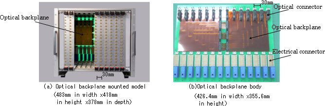
Figures 2 Optical backplane with 3 tera-bits per second
|
The optical backplane must be connected to a board loaded with a large number of optoelectronic circuits inside a narrow pitch of about 30 mm. When these boards are connected with the optical backplane, light must be bent through a right angle. The system of using the mirror and the lens as the right-angled redirection has already been published, but difficulties related to the large number of optical connections involved as well as the large connection loss remained unsolved.
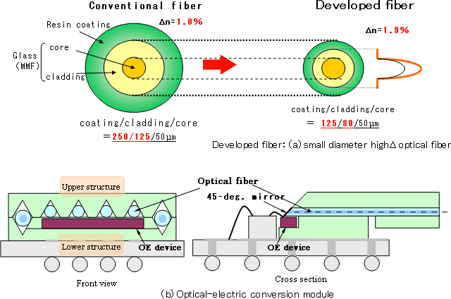
The AIST group use the connection method developed at ASET to bend the optical fiber through a right angle in the range of no los to develop the technologies for a compact and easy to assemble structure. The key technologies for this system consist of development of high density optical connection parts and compact fiber bend right-angled optical connector that allow coupling of small diameter (125 µm) high Δ optical fiber, half the diameter of conventional fibers, with 16 optical fibers at one time (Figure 3-a). In addition, an optical-electric conversion module (Figure 3 - (b)) able to send and receive the optical signal of 10 giga-bits per second has been developed, installed on the board, and its performance has been confirmed.
 |
|
Figure 3 Small diameter high Δ optical fiber (a) and optical-electric conversion module (b)
|
In the small diameter high Δ optical fiber without coating removal, the refractive index ratio of cladding to core is enlarged ensuring that there is no optical loss even at the small bending radius required to fit the optical connections into the narrow pitch. Furthermore, the 125 µm diameter of the glass fiber, including the protecting resin layer, is accurately kept, and the fiber can be directly coupled to standard optical connection parts without coating removal.
The structure of the newly developed optical connecting parts is divided into two sections: the section inserting the fiber tips polished previously, and the section fixing the aligned fiber boards. This structure makes it possible to connect high density optical fibers in the 30 mm narrow pitch.
As for the small-sized fiber bend right-angled optical connector, the backplane and the inserted switching board can be assembled in a small space. Compared to other research works, the external size of the developed optical connector has been reduced to one third of that of recently reported structures.
To fabricate the optical-electric conversion module for interconnecting to this optical backplane, the upper structure, which has been formed into a mirror by fixing four fibers array and cutting their edges at an angle of 45 degrees, is assembled upon the lower structure where the optoelectronic device is mounted. The optoelectronic device and fiber array are coupled to produce a 90-degree redirection in the optical path and to achieve optical integration. As for assembling upper and lower structures, instead of precise optical axis alignment using the conventional method of passing light through the fiber, a simple procedure that uses mechanical alignment and mutual alignment of the marks has been developed to build the low-cost backplane system.